
Antennas
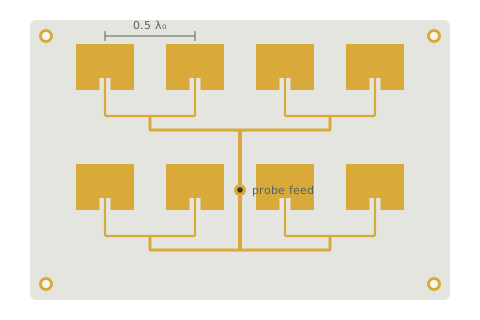
Patch and slot antenna arrays
Microstrip patch, slot and series-fed arrays for base stations, radar and satellite terminals.
RF and microwave PCB manufacturer
Rogers, Taconic, Isola and PTFE laminates from prototype to production. Every quote is reviewed by an RF engineer and comes back with a DFM report.
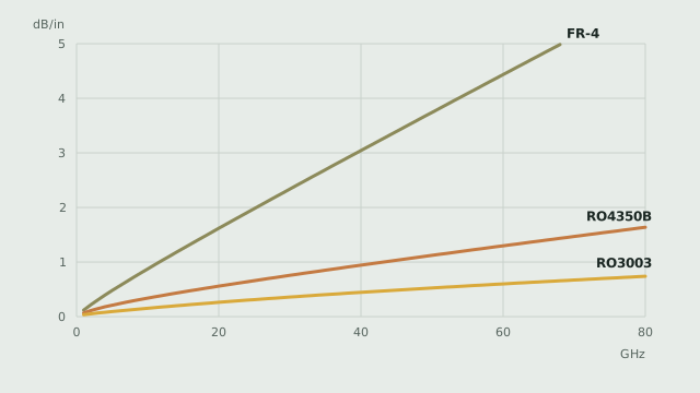
Insertion loss, 50 Ω microstrip
GHz
Per 100 mm on a 0.508 mm core, 1 oz copper, datasheet Df and foil roughness. Hatched: above the laminate's rated range.
Size your own line in the impedance calculatorLaminates in stock from
Design Dk, loss and rated frequency for the laminates engineers ask us for most. Every row opens a full datasheet with fabrication notes.
| Laminate | Dk design | Df | Loss @ 28 GHz | Rated to | Cost |
|---|---|---|---|---|---|
| High-Tg FR-4 FR-4 | 4.30 | 0.0170 | 8.64 dB* | 6 GHz | |
| RO4350B Rogers | 3.66 | 0.0037 | 2.82 dB | 30 GHz | |
| RO4003C Rogers | 3.55 | 0.0027 | 2.39 dB | 30 GHz | |
| Astra MT77 Isola | 3.00 | 0.0017 | 1.65 dB | 81 GHz | |
| RO3003 Rogers | 3.00 | 0.0010 | 1.33 dB | 81 GHz | |
| RT/duroid 5880 Rogers | 2.20 | 0.0009 | 1.07 dB | 81 GHz |
Loss per 100 mm of 50 Ω microstrip on a 0.508 mm core with 1 oz copper, including foil roughness. * above the laminate's rated range.
From single-layer patch arrays to 16-layer hybrid beamformers. Each page lists tolerances, recommended laminates and the checks we run.
Antennas
Microstrip patch, slot and series-fed arrays for base stations, radar and satellite terminals.
Passive networks
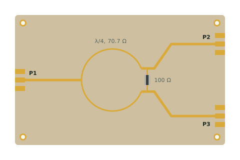
Two-way and N-way Wilkinson dividers with chip or printed isolation resistors.
Passive networks
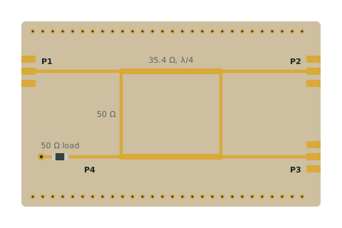
Branch-line hybrids, rat-race couplers and edge- or broadside-coupled stripline couplers.
Passive networks
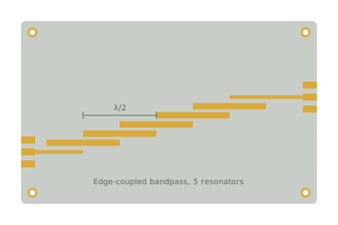
Edge-coupled, hairpin, interdigital and SIW filters with tight resonator control.
Active boards
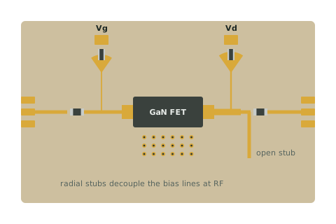
Power amplifier and low-noise amplifier boards with thermal management built into the PCB.
Active boards
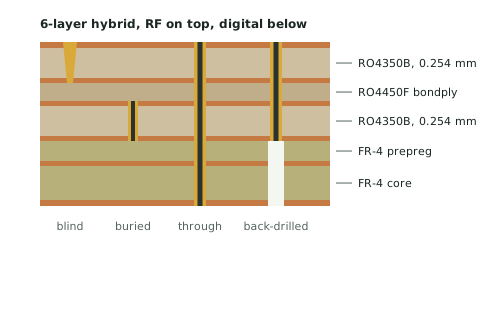
Multilayer hybrid boards that combine RF antenna layers, stripline distribution and digital control.
The same laminates, tuned to very different constraints: PIM on base-station antennas, phase stability in radar, outgassing in space.
Telecom
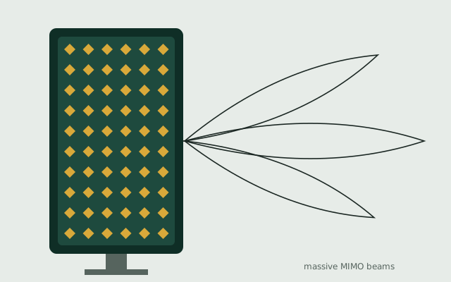
Massive MIMO antennas, power amplifiers and filters for macro and small-cell base stations.
Automotive
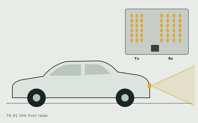
Front, corner and imaging radar boards with series-fed patch arrays on thin low-loss layers.
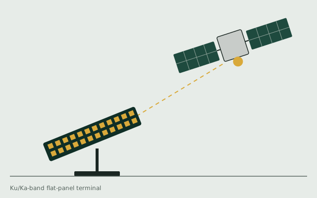
Space and satcom
Flat-panel terminal antennas, LNB front ends and beamforming layers for Ku and Ka band.
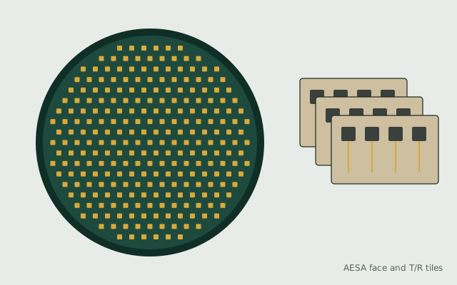
Aerospace and defence
AESA radar tiles, EW receivers and airborne antennas built to IPC-6018 Class 3.
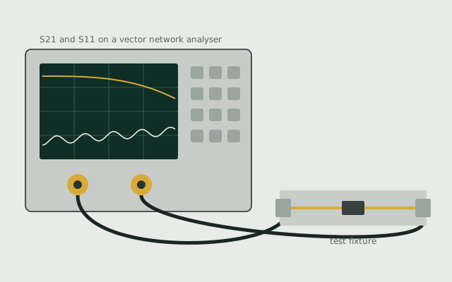
Test and measurement
Test fixtures, calibration boards, probe interfaces and load boards for RF and high-speed digital.
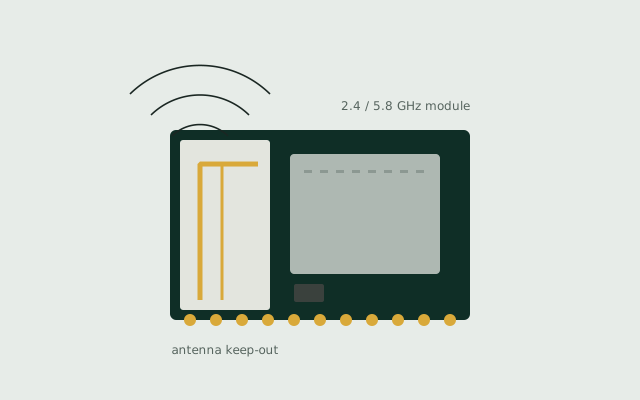
Consumer and IoT
Wi-Fi, UWB, GNSS and LPWAN modules with integrated antennas and tight cost targets.
Size a line, shortlist a laminate, estimate a price. Every result carries straight into a quote request.
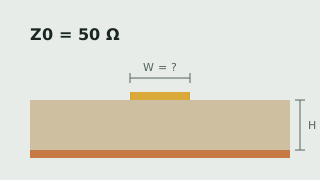
Trace width for a target impedance, effective Dk, guided wavelength and a loss estimate, for any laminate in the database.
Open tool
Answer four questions about frequency, circuit, priority and stackup to get a ranked laminate shortlist.
Open tool
An indicative price range from material, layer count, size, quantity, finish and lead time.
Open toolBuilt for RF tolerances, not adapted from a digital line.
| Layer count | 1 to 24 layers, hybrid up to 16 |
|---|---|
| RF laminates | Rogers, AGC (Taconic), Isola, Panasonic, Wangling |
| Minimum trace and space | 0.075 mm / 0.075 mm (3 / 3 mil) |
| RF etch tolerance | ±0.02 mm on controlled layers |
| Impedance tolerance | ±5% with TDR coupons, ±10% standard |
| Board thickness | 0.1 to 6.0 mm |
| Surface finishes | Immersion silver, ENIG, ENEPIG, immersion tin, OSP, hard gold |
| Special processes | Cavities, copper coin, metal backing, back-drilling, edge plating, via-in-pad |
| Test and inspection | Flying probe, TDR, AOI, X-ray, microsection |
| Build standards | IPC-6012 and IPC-6018, Class 2 or Class 3 |
Gerber or ODB++, drill file, stackup and target impedances. A PDF drawing helps.
An RF engineer checks etch compensation, stackup, material stock and tolerances, and sends a report with the quote.
Lamination, drilling, PTFE hole treatment, plating and imaging with per-panel etch compensation.
Electrical test on every board, TDR on impedance coupons, and microsections per lot.
Vacuum packed with test report, certificate of conformance and laminate lot certificates.
Short, practical notes on laminates, stackups and mmWave layout, written by the people who build the boards.
Materials
Same resin family, same FR-4-like processing, different loss and flame rating. How to decide in two questions.
Manufacturing
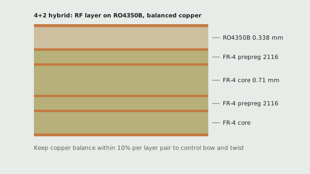
Putting RF laminate only where the RF runs saves money. Keeping the board flat takes symmetry, the right bondply and a lamination plan.
Design
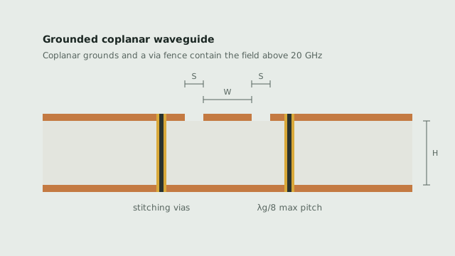
Microstrip is easy until it starts to radiate. What grounded coplanar waveguide fixes, what it costs, and how tight the via fence has to be.
Every lot ships with electrical test data, TDR coupon results, microsection images and laminate certificates.
Send Gerbers or ODB++ with your stackup and impedance targets. An RF engineer replies with pricing, material availability and a DFM report.